
School of Microelectronics, Xidian University, Xi’an, China.
*Corresponding author : Guangbao Shan
School of Microelectronics, Xidian University, Xi’an, China.
Email: gbshan@xidian.edu.cn
Received: Oct 18, 2024
Accepted: Nov 22, 2024
Published Online: Nov 29, 2024
Journal: Journal of Artificial Intelligence & Robotics
Copyright: © Shan G (2024). This Article is distributed under the terms of Creative Commons Attribution 4.0 International License.
Citation: Li G, Shan G, Zheng Y, Meng B, Cao H. The application of machine learning methods in the design of electronic systems for robotics. J Artif Intell Robot. 2024; 1(2): 1015.
This article provides a comprehensive review of the application of Artificial Intelligence (AI) in the design and optimization of microsystem integrated circuits, particularly for robotic systems. The study covers AI-based methods for both single-field and multi-field designs, focusing on the challenges of optimizing electromagnetic, thermal, and mechanical performance in compact, highly integrated systems. Additionally, the use of Physics-Informed Neural Networks (PINNs) is highlighted for improving the accuracy of multi-field simulations while reducing computational costs and data requirements. The main findings emphasize the advantages of combining AI with physical principles to enhance design efficiency, improve prediction accuracy, and minimize data usage in the development of advanced microsystems.
Keywords: Artificial Intelligence (AI); Microsystem design; Physics-Informed Neural Networks (PINNs); Robotics.
With their advantages in convenience, efficiency, and autonomous operation, robots have found widespread applications across various fields, including healthcare, engineering machinery, ocean exploration, aerospace, and agriculture [1,2]. Integrated Circuits (ICs), as the core component of robotic control systems, are crucial in determining whether a robot can successfully perform in complex terrains and high-demand work environments. In recent years, the rising demand for small-scale robots has driven IC development toward miniaturization, high performance, and enhanced reliability. However, as Moore’s Law gradually loses its effectiveness, the traditional method of improving IC integration by reducing feature size has become less viable. This shift has made three-dimensional (3D) ICs a promising path for achieving miniaturization and improved performance. With 3D integration, coupled multi-field effects become more pronounced in limited volumes, and as technology advances, the complexity and precision required in design continue to increase [1-3].
Traditional IC design processes often depend heavily on manual input, making them both time-consuming and error-prone2 [1]. With rapid advancements in machine learning, deep learning, and algorithm optimization, intelligent design tools have become a major trend in the IC design domain. By incorporating intelligent design techniques, design automation tools can significantly enhance design efficiency, improve quality and accuracy, reduce design cycles, and cut costs. Synopsys, an industry leader in Electronic Design Automation (EDA), has launched DSO.ai, the first AI-driven design tool in the EDA sector, enabling the successful design of several micro-systems. Similarly, Cadence has introduced the JedAI platform, which represents a technological shift in EDA by leveraging past design experiences and applying artificial intelligence to optimize future designs, specifically in Power, Performance, and Area (PPA). Additionally, Google has utilized AI to optimize the physical layer of chips. The rapid evolution of AI is revolutionizing microsystem design methodologies, driving a transition from traditional human-led analysis and optimization to AI-driven, data-centric intelligent design approaches in microsystems.
The convergence of robotic technology and intelligent IC design opens up new possibilities for the future of automated and intelligent systems [1]. By leveraging AI’s non-linear, adaptive, and self-learning capabilities to understand the relationships between IC design parameters and outputs, end-to-end intelligence can be achieved from functional design to physical implementation, greatly enhancing system flexibility and adaptability [1,2]. Machine learning-based optimization methods are especially valuable when system complexity rises, requiring simultaneous optimization of numerous input parameters, as is often the case with 3D ICs and complex systems [1,2]. Furthermore, intelligent design tools aid engineers in identifying hidden design flaws within intricate environments, offering intelligent decision support and enabling the creation of high-performance, highly reliable ICs [1,2].
The intelligent single-field and multi-field design of microsystems is a crucial component of integrated microsystem design, yet a systematic summary of methods and corresponding application scenarios is lacking. This paper focuses on summarizing the applications of artificial intelligence technology in single-field and multi-field microsystem design, as illustrated in (Figure 1). The main contributions of this paper are as follows: (1) The application of traditional artificial intelligence methods in single-field microsystem design is summarized; (2) The application of traditional artificial intelligence algorithms in integrated multi-field microsystem design is reviewed. (3) The use of AI methods combined with physical equations in multi-field microsystem design is examined; (4) the characteristics and application scenarios of various methods are comparatively discussed. This work provides a valuable reference for efficient, rapid, and intelligent integrated microsystem design in the future.

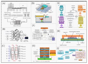
The development of 3D microsystem technology has significantly advanced robotics by providing effective solutions to enhance electronic system performance while reducing size [1]. However, challenges persist in microsystem design, including signal crosstalk, substantial thermal accumulation, and complex stress distribution, all of which impact overall microsystem performance [2]. To address these issues, researchers have integrated various machine learning methods to optimize microsystem and component design for tasks such as eye diagram prediction [3], crosstalk analysis, frequency domain analysis, parasitic parameter extraction, and temperature and stress distribution [4,5], thereby improving modeling efficiency.
After robotic integration, various electromagnetic devices are incorporated into compact volumes, making crosstalk issues between components more pronounced and increasing the complexity of parasitic parameter interactions. As a result, many researchers have integrated neural networks with evolutionary methods to improve the electrical performance of these designs. To address the time-intensive nature of traditional Monte Carlo modeling methods and the over-design associated with worst-case scenarios, [4] proposed an eye diagram prediction model based on Deep Neural Networks (DNN), and the concept of the proposed channel characteristic-based DNN model is shown in (Figure 2A). Compared to other regression methods, the proposed method reduced the error rates of eye height and eye width by 22.7% and 43.9%, respectively, while also lowering computational costs by 8.0%-9.4%. To reduce the amount of labeled data. Proposed [4] a rapid training semi-supervised learning method based on a Hybrid Neural Network (HNN) to predict eye diagram metrics, and the proposed method is shown in (Figure 2B). This method reduces the labeled training data by 50%, improving the prediction accuracy of eye height and eye width by 32.29% and 33.55%, respectively. Optimizing crosstalk in high-speed interconnect structures is crucial for accurate signal transmission in integrated circuits [4]. Developed [4] an artificial neural network model to predict near-end and far-end crosstalk in coupled microstrip transmission lines. Proposed [4] a neural network-based rapid prediction method for RLGC matrices of microstrip lines, and the ANN model for channel RLGC components is shown in (Figure 2C), achieving a prediction error of less than 5%. Additionally, genetic algorithms have been used to optimize transmission line loss and crosstalk, with the optimized parameters subsequently verified through CST electromagnetic simulation models. Proposed [4] a bonding line interconnect performance optimization method that combines neural networks and genetic algorithms, and the diagram of the presented bonding-wire compensation structure is shown in (Figure 2D). The optimization time is reduced from 7.63 hours to 0.2 hours and significantly enhancing efficiency. At the same time, the high integration density of microsystems within miniature robots exacerbates thermal accumulation effects in compact volumes, while the complexity of heat dissipation structures rapidly increases. Consequently, intelligent thermal design technologies based on neural networks and evolutionary methods have proven particularly valuable for minimizing computational resource use and time costs during optimization. Introduced [4] a hybrid prediction method for microchannel cooling performance that combines artificial neural networks with genetic algorithms, particle swarm optimization, and other algorithms such as artificial hummingbird and zebra algorithms. The workflow of all models is shown in (Figure 2E), and the model, trained on six critical microchannel input parameters, used heat resistance and pumping power as target outputs, reducing average errors for heat resistance and pumping power by 88.7% and 81.4%, respectively. Developed [4] a convolutional neural network-based method for predicting anisotropic equivalent thermal conductivity, and the framework of the proposed method is shown in (Figure 2F). This model achieves highly accurate predictions of the effective thermal conductivity of semiconductor packaging substrates within 2-3% error, thereby reducing human uncertainty and labor requirements. Introduced [4] a modeling method that combines genetic algorithms with computational fluid dynamics (CFD) to improve cooling efficiency through geometric modifications. By optimizing plate fin heat sinks using multi-objective genetic algorithms and CFD simulations, they achieved a 65% reduction in thermal accumulation. Developed [4] a microchannel control method that combines Bayesian optimization and artificial neural networks, mapping microchannel flow rates with power and temperature, and schematic of a 3-D IC with integrated MFHS is shown in (Figure 2G). This approach intelligently reduces pump power consumption while maintaining the temperature limits of 3D integrated circuits using microfluidic coolers and layered cooling. With the integration of microsystems, diverse materials are compacted into small volumes, creating significant stress issues due to varying thermal expansion coefficients and substantial thermal accumulation. To predict stress distribution within microsystems rapidly, researchers have explored intelligent stress design methods for interconnect structures and packaging [4]. At IBM have pioneered AI-Design for Reliability (AI-DfR), which utilizes neural networks to predict wafer-level chip-scale package (WLCSP) solder joint fatigue life. Cross-section of a module level flip-chip package is shown in Figure 2H. Similarly, developed [4] an artificial neural network model trained on a database generated through finite element analysis for predicting WLCSP solder joint fatigue life, achieving over 90% accuracy and incorporating solder creep material models. Proposed [4] a three-dimensional board-level drop response model for Ball Grid Array (BGA) package structures based on a backpropagation neural network, and the calculation flow of the BP neural network structure is shown in (Figure 2I). Compared to traditional finite element simulations, the proposed method improves computational efficiency by more than three orders of magnitude. Proposed [4] a rapid prediction method for runtime reliability management using artificial neural networks. This method leverages temperature and stress data for offline training to develop a neural network-based stress model. The prediction error is less than 7% when compared with finite element method errors.
| Ref | Application | Method | Input | Output |
|---|---|---|---|---|
| [19] | Predict and optimize eyediagrams | DNN | Geometric parameters of channel | Eye heightand eye width |
| [20] | Predict interconnected eye diagrams | DNN+CNN | Channel geometry parameters | Eye heightand eye width |
| [22] | Predict coupledtransmission line crosstalk | ANN | Transmission line geometric parameters | Near-end crosstalk, far-end crosstalk |
| [23] | Predict the microstrip lineRLGC | ANN | Transmission line geometric parameters | RLGC matrixof the channel |
| [24] | Predict and optimize wire-Bonding Compensation Structure | ANN+GA | Structure parameters | Operating frequency |
| [25] | Predict and optimize microchannel thermal resistance and pumping power | ANN+GA, PSO,AHA, ZOA | Geometric parameters of the microchannel | Thermal resistance, pumping power |
| [26] | Predict the anisotropic equivalent thermal conductivity of the package | CNN | Substrate material properties, material location | Equivalent thermal conductivity |
| [27] | Optimize the efficiency of finned heatsinks | GA | Geometric parameters of the heatsink | Efficiency of finned heatsinks |
| [28] | Optimize the pumppower of the microfluidic heatsink | ANN+BO | Temperature at time“t−1” Power at time “t” andFlow rate at time “t | Pump power consumption and temperature |
| [29] | Predict packagemechanical behavior | ANN | Laminate chip-site CTE, Laminate fan-out CTE, Die to sealband distance_x, Die to seal-band distance_y, Stress free temperature | Die corner shear stress, Die principal stress, TIM strain, Maximum laminate Warpage, Sealband peeling stressand Laminate warpage nodaloutput |
| [30] | Predict maximum creepstrain and fatigue life of wafer-level chip scale packages | ANN | Chip thickness, PCBthickness, and solderpitch | Maximum creepstrain and fatiguelife |
| [31] | Prediction board levelBGA impact corresponding life | ANN | Node dropAngle, x, y, and z coordinates | von Mises stress, PEEQ, warping deformation, energy density of nodes |
| [32] | Predictive stress | ANN | The temperature around each TSV | Maximum stress |
The above discussion highlights the application of neural networks and evolutionary algorithms in addressing electromagnetic, thermal management, and stress challenges in miniature robots, focusing on solving issues such as crosstalk, thermal accumulation, and stress due to the high integration density of components, with a detailed comparison shown in (Table 1). In electromagnetic design, researchers have combined neural networks and genetic algorithms to optimize transmission lines, crosstalk, and loss, significantly reducing computation time and errors. Additionally, these techniques have been widely applied to thermal management and stress prediction, such as through microchannel cooling models, heat sink optimization, and stress design, leading to significant improvements in cooling performance and stress prediction accuracy. Overall, the integration of neural networks and evolutionary algorithms demonstrates substantial potential in reducing computation time, minimizing data requirements, and enhancing design efficiency.
In the single-field intelligent design of microsystems, researchers have achieved rapid prediction and intelligent optimization of electrical performance, thermal distribution, and stress distribution. However, as microsystem dimensions shrink, integration levels increase, and signal transmission frequencies rise, the interactions and couplings between multiple physical fields within a small volume become crucial factors affecting the overall performance of microsystems. Moreover, due to the coupling of these physical fields, traditional numerical methods often require extensive resources and costs to solve, while conventional equivalent modeling methods encounter difficulties in accuracy and modeling complexity. Consequently, research on intelligent multi-field design methods for microsystems based on machine learning has gradually emerged.
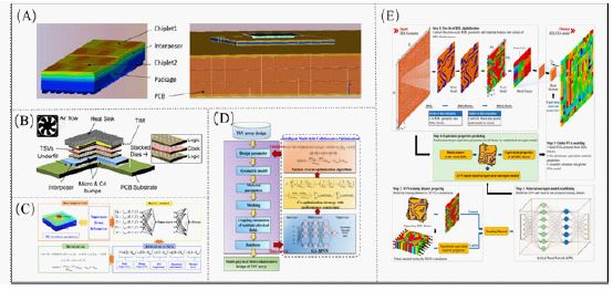
ANSYS introduced a new EDA platform that utilizes machine learning-assisted methods to achieve design and optimization of temperature and IR drop in three-dimensional integrated circuits (3D ICs), system testcase with thermal heatmap and assembly stackup is shown in (Figure 3A) [4]. Proposed [4] an electro-thermal-mechanical coupling M3D array design method based on artificial neural networks. Compared with standard BP neural networks, the threshold and weight prediction models in this approach demonstrated superior advantages in both prediction time and accuracy. Used [4] a combination of machine learning and Bayesian optimization algorithms for simulating and optimizing the electrothermal performance of three-dimensional integrated circuits and systems, Configuration of a 3-D system for optimization is shown in (Figure 3b). By taking five design parameters as input variables and outputting the maximum temperature, temperature gradient, and weighted clock skew, this approach reduced computation time by 31.1% compared to traditional simulation methods, with optimization results showing superior performance relative to other methods. However, Park’s approach requires lengthy numerical simulations with each iteration, resulting in extended optimization time.
Proposed [4] a multi-objective optimization method for the thermal stress of TSV arrays, combining BP neural networks with Particle Swarm Optimization (PSO), flowchart of the developed intelligent optimization method for the parameters of TSV is shown in (Figure 3C). This method optimizes the temperature, stress, and thermal expansion deformation of TSV arrays, reducing simulation time from 2 hours to 70 seconds. Proposed [6] an intelligent multi-field collaborative optimization method for TSV arrays, using datasets obtained from finite element methods and a Genetic Algorithm-Based Backpropagation Neural Network (GA-BPNN) to establish a mapping relationship between the design parameters and performance parameters of TSV arrays, developed method flowchart is shown in (Figure 3D). Under performance constraints, they utilized particle swarm optimization for multi-field collaborative optimization. Simulation results indicated that the maximum deviation was only 3.04%, and, compared to traditional methods, search and computation times were reduced by 99.52% and 83.86%, respectively. Established [4] a finite element model of a 3D IC device with inner pin microchannels and full-copper interconnections, performing simulations and applying the RSA method for multivariate nonlinear fitting of the results. This produced an RSA surrogate model of the objective function, verified for accuracy. The model was solved and optimized using the NSGA-II program in MATLAB, achieving design parameters for optimal solutions A and B, which reduced resistance by 86.4% and maximum stress by 29.4%. From [4] ASE, explored the potential of neural networks in predicting warpage in fan-out wafer-level packaging. Ante proposed [4] a microchannel design method based on multi-objective optimization algorithms that can accurately predict the optimal microchannel heat sink design. Compared to traditional optimization methods, this approach achieved more than a 10% reduction in temperature and over a 25% reducti on in pressure. Additionally, [4] proposed an RDL modeling simulation method based on machine learning, the overall ANN modeling flow is shown in (Figure 3E). Using neural networks to construct equivalent material models of subsets, they transformed all subsets into elements for temperature and stress simulation, achieving a maximum error of 2.81%. This approach accurately considers layout impacts in advanced packaging design, enhancing design reliability with minimal resource utilization.
In summary, the integration of machine learning and optimization algorithms into the design and analysis of 3D integrated circuits and packaging has led to significant advancements in accuracy, efficiency, and overall system performance. The use of neural networks, genetic algorithms, and Bayesian optimization has shown promising results in reducing computation times and improving the prediction of key metrics such as temperature, stress, and warpage, with a detailed comparison shown in (Table 2). These intelligent design methods offer clear advantages over traditional approaches, particularly in handling the complexity of multi-physical field interactions in advanced microsystem structures. As a result, machine learning-assisted methods are becoming essential for achieving optimal design outcomes while minimizing resource use.
| Ref | Application | Method | Input | Output |
|---|---|---|---|---|
| [33] | Predict and optimize 3D IC temperature and IR drop | - | Geometric parameters of the chip | Temperature and IR drop |
| [34] | Predicting theM3D array multifield distribution | ANN | Temperature of monolithic inter-tiervias | Max stressof monolithic inter-tiervias |
| [35] | Predict and optimize the peak temperature, time jitter of the3D IC | ANN+ Bayesian | Air velocity, material thickness, type | Maximum temperature, temperature gradient, clock jitter |
| [36] | Predict and optimize the thermal stressof TSV arrays | BPNN+PSO | Radius, silica thickness, and pitch of TSVS | Maximum stress, peak temperature, displacement |
| [6] | Predict and optimize the multifield performance of TSV arrays | GA-BPNN+PSO | Radius, height, oxidethickness, pitch, and offsetAngle of TSV | S-parameter, peak temperature, peakstress |
| [37] | Predict and optimize the resistance and stress of the microchannel and copper interconnection | Response surfaceapproximation + MOEA | Radius, microbump thickness, and microbumpheight of TSV | Maximum thermal stress, TSV conductivity |
| [38] | Predicting the warping of wafer-level packages | ANN+ Bayesian | Chip CTE, fan-outCTE, chip position, package stress-free temperature | Shear stress, principal stress, material strain, warping degree |
| [39] | Predict and optimize microchannel heat dissipation and stress | ANN | Structural parameters of the microchannel | Peak temperature, stress |
| [40] | Predict the temperature andstress of the RDL layout | ANN | RDL subset | Temperature, maximum stress |
In the design of microsystems, the integration of physics-informed approaches has become increasingly important to accurately capture complex multi-physics interactions that are difficult to represent with purely data-driven models. Physics-informed methods embed domain-specific knowledge directly into the modeling process, ensuring that solutions are consistent with fundamental physical laws, and overcoming limitations posed by traditional machine learning methods, which may not fully account for physical principles.
In the design of microsystems, the integration of physics-informed approaches has become increasingly important to accurately capture complex multi-physics interactions that are difficult to represent with purely data-driven models. Physics-informed methods embed domain-specific knowledge directly into the modeling process, ensuring that solutions are consistent with fundamental physical laws, and overcoming limitations posed by traditional machine learning methods, which may not fully account for physical principles.
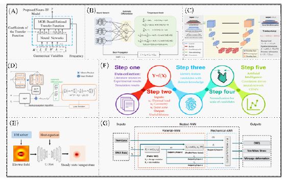
To address this, researchers have recently developed neural network models driven by domain knowledge to ensure that solutions adhere to corresponding physical principles. Proposed [4] a neural network combined with transfer functions to achieve rapid characterization of the amplitude-frequency response of interdigital band-pass filters, the structure of the proposed MOR-based neuro-TF model is shown in (Figure 4A), yielding a testing error of only 0.78%. Introduced [4] a neural network framework incorporating electromagnetic domain knowledge, using a quadratic approximation method to extract poles and residues, and subsequently employed the established neural network framework for the rapid characterization of microwave devices, achieving a testing error of 1.60%. Proposed [4] a thermal distribution prediction model for microsystems based on a physics-informed neural network, the overall architecture of the proposed PINN is shown in (Figure 4B). Fast prediction of heat sink heat distribution is achieved by data-free simulation, and the simulation results are consistent with the actual reference data. Proposed [4] a 3D CNN model based on the heat transfer equation to predict the thermal response of FC-BGA packaging. The proposed the physical-based deep learning model is shown in (Figure 4C). The proposed model can rapidly and accurately predict the temperature distribution of FC-BGA models with various materials and complex structures. The solution speed of the proposed model is more than 400 times faster than that of the finite element model. Proposed [4] a fast full-chip numerical analysis method using an enhanced Physics-Informed Neural Network (PINN) framework, which is shown in (Figure 4D), enabling design space exploration and uncertainty quantification. The solution speed of the physics-informed neural network for the heat equation, considering both training and inference time, is more than six times faster than COMSOL, with an average absolute error of 0.47 K. Proposed [4] a novel Physics-Informed Neural Network (PINN)-based method to construct a multi-physics solver, establishing a fast characterization framework combining FDTD and PINN to accurately represent multi-physics field distributions, and the proposed model is shown in (Figure 4E). Developed [4] the traditional ANN into their newly proposed Correlation Drive Neural Network (CDNN) for predicting solder joint fatigue and creep, and the schematic describing the process of the proposed correlation-driven neural network is shown in (Figure 4F). Proposed [4] a physics-based nested neural network model consisting of a material neural network and a mechanical neural network for predicting the solder joint lifespan of fan-out WLCSPs and the proposed physics-based nested-ANN model is shown in (Figure 4G). The model calculates equivalent strain, von Mises stress, and deformation based on material coefficients and geological material properties, with a computation time of 13.2 seconds, improving work efficiency, reducing computation time, and accelerating packaging reliability assessment.
| Ref | Application | Method | Input | Output |
|---|---|---|---|---|
| [42] | Prediction of frequency domain response of an interdigital bandpass filter | Neuro-TF | Geometric dimensions and frequency of the filter. | Frequency domainresponse |
| [43] | Predicting the frequency domain response of a waveguide filter | Neuro-TF | Geometric dimensions and frequency of the filter. | Frequency domainresponse |
| [44] | Predicting the temperature distribution of a microprocessor. | PINN | Temporal and spatial information of microprocessor | Transient temperature distri-bution |
| [45] | Predicting the thermal response of the FC-BGA package | PINN | Voxel model withmaterial property tensors and initial field tensor, interior points tensorwith one material and boundarypoints with boundary condition | Thermal field difference quotient |
| [46] | Predicting the full chipthermal response | ThermPINN | Ambient temperature effective convection coefficient | Temperature |
| [47] | Arbitrary shape lossdielectrics and steady-state temperature distribution | PINN | Dissipated power density from FDTD and domain properties | Steady-state temperature distribution (T) |
| [48] | Predicted lifeof solder jointsof electronic devices | CDNN | Thermal load,geometric parameters, jointzone | Creep orfatigue |
| [49] | Predict thesolder joint lifeof fan-out WLCSPs | PINN | Material coefficient, geological material properties | Equivalent strain, vonMises stress, anddeformation |
In summary, the integration of domain knowledge into neural network models has greatly improved the accuracy and efficiency of simulations in fields such as electromagnetic characterization, thermal prediction, and mechanical stress analysis. These models, including physics-informed neural networks, have demonstrated remarkable speed and precision in predicting complex behaviors, such as temperature distribution in FC-BGA packaging and fatigue in solder joints with a detailed comparison shown in (Table 3). By embedding physical principles into the models, researchers have been able to significantly reduce computation time while maintaining high accuracy, making these techniques highly effective for optimizing the performance and reliability of various microsystems.
From the design examples discussed in this paper, it is evident that artificial intelligence methods have been widely applied in single-field and multi-field pre-optimization and prediction for integrated circuits in robotics. In multi-field design contexts, traditional machine learning techniques have primarily been used for applications such as high-speed signal eye diagrams, crosstalk, parasitic parameters, frequency response in electrical fields, maximum temperature, thermal resistance, pumping power, equivalent thermal conductivity, and thermal response in thermal fields, as well as stress and solder joint fatigue life in stress fields. Due to the structural limitations of traditional neural networks, these methods are often focused on predictions and optimizations of limited, specific performance metrics in integrated circuits. While they have, to some extent, replaced traditional numerical and equivalent methods, balancing prediction accuracy with design efficiency, they generally lack physical interpretability and often produce physically inconsistent singular points during prediction, requiring large datasets for training. Physics-informed neural networks (PINNs), which incorporate physical information in transfer functions and loss functions, significantly enhance the interpretability and generalizability of prediction results. They also greatly reduce the dependency on training data, potentially eliminating the need for a training set altogether. This substantially improves both the interpretability and predictive accuracy of neural networks. PINNs are often applied in scenarios involving broadband frequency domain responses, temperature and stress distributions across entire solution domains, and solder joint fatigue life, providing enhanced spatial solving capabilities and time-frequency domain dimensionality reduction.
Looking ahead, as robots and electronic systems continue to shrink in size, multi-field coupling effects will become even more pronounced, and balancing trade-offs between multiple software iterations and performance metrics will increase in complexity, reducing the efficiency of traditional analysis methods. While traditional neural networks and PINNs have demonstrated developmental potential in multi-field coupling design by significantly improving design efficiency with minimal sacrifice in solution precision, several challenges remain:
Modeling challenges with complex geometries: As electronic system designs become increasingly complex, geometries will grow more intricate. PINNs must encode PDEs and boundary conditions into the loss function, and the priority of multiple loss functions during training requires careful weighting to ensure efficient model training.
Inverse design: Currently, most research focuses on predicting performance parameters based on design parameters. However, real-world engineering problems often require performance specifications first, followed by determination of design parameters. Developing inverse design methods to address these needs is crucial.
Cross-scale issues: The complexity of electronic system design spans multiple scales, and leveraging PINNs for cross-scale training involves balancing prediction accuracy with prediction time. Rapidly predicting physical field distributions using small sample data is especially important.
This paper presents the application of AI technologies in the performance prediction and optimization design of microsystem integrated circuits. It summarizes and compares the use of AI in the single-field and multi-field design of microsystems for robotics, as well as the application of physics-informed neural network methods in the multi-field design of robotic microsystems. Finally, various machine learning methods are discussed and compared. The main conclusions are as follows:
Neural networks can be used for the rapid prediction and optimization of single-field and multi-field performance of microsystems; however, ensuring prediction accuracy requires a large amount of data to train the neural networks.
The combination of neural networks and heuristic optimization algorithms can accelerate multi-field optimization design for microsystems, reducing iteration time at each step.
Physics-informed neural networks ensure that the prediction results meet physical constraints, while further reducing the amount of required data and improving both prediction accuracy and generalization capabilities.
Funding: This work is supported in part by the National Key Research and Development Program of China (No. 2022YFB4401302), Science Fund for Creative Research Groups of the National Natural Science Foundation of China (No. 62021004).